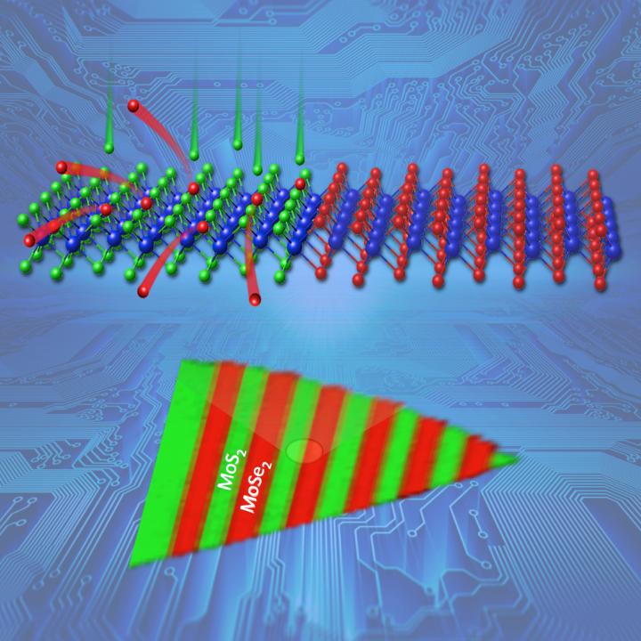
Ultrathin electronics could soon be developed as researchers have developed a novel way of producing arrays of semiconductor junctions within a single, nanometer-thick semiconductor crystal.
Currently available transistors may be miniscule – just 10 nanometers wide – but they are formed from 3D crystals and hence are not ideal for ultrathin electronics. Researchers working on developing ultrathin electronics have long been looking at 2D crystals as one of the options and though they have been able to lithographically pattern single layers of carbon atoms called graphene into ribbon-like “wires” with insulation by a similar layer of boron nitride, they haven’t been able to come up with a synthesis and processing mechanism that can lithographically pattern junctions between two different semiconductors within a single nanometer-thick layer to form transistors.
This is what researchers at the Department of Energy’s Oak Ridge National Laboratory have achieved by combining a novel synthesis process with commercial electron-beam lithography to produce arrays of semiconductor junctions in arbitrary patterns within a single, nanometer-thick semiconductor crystal.
The newly developed process relies upon transforming patterned regions of one existing, single-layer crystal into another.

CREDIT
Oak Ridge National Laboratory, U.S. Dept. of Energy
The process involves growing single, nanometer-thick layers of molybdenum diselenide crystals on substrates followed by depositing of protective patterns of silicon oxide using standard lithography techniques. After this, the exposed regions of the crystals are bombarded with a laser-generated beam of sulfur atoms. The sulfur atoms replaced the selenium atoms in the crystals to form molybdenum disulfide, which has a nearly identical crystal structure. The two semiconductor crystals formed sharp junctions, the desired building blocks of electronics.
“We can literally make any kind of pattern that we want,” said Masoud Mahjouri-Samani, who co-led the study with David Geohegan. Geohegan, head of ORNL’s Nanomaterials Synthesis and Functional Assembly Group at the Center for Nanophase Materials Sciences, is the principal investigator of a Department of Energy basic science project focusing on the growth mechanisms and controlled synthesis of nanomaterials.
Millions of 2D building blocks with numerous patterns may be made concurrently, Mahjouri-Samani added. In the future, it might be possible to produce different patterns on the top and bottom of a sheet. Further complexity could be introduced by layering sheets with different patterns.
“The development of a scalable, easily implemented process to lithographically pattern and easily form lateral semiconducting heterojunctions within two-dimensional crystals fulfills a critical need for ‘building blocks’ to enable next-generation ultrathin devices for applications ranging from flexible consumer electronics to solar energy”, added Geohegan.
The findings have been published in Nature Communications.
